Imaging and spectroscopy
We use advanced imaging methods to evaluate the morphological, chemical, and transport properties of membranes and electrodes. For instance, the porosity of the electrode within a membrane electrode assembly can be investigated by 3D imaging using scanning electron microscopy, and the degree of chemical degradation of a membrane after fuel cell operation can be quantified by confocal Raman microscopy. Here, we provide an overview of the microscopes and spectroscopic techniques that we employ to characterize membranes and membrane electrode assemblies.
Optical microscopy and Raman spectroscopy
Optical microscopy is a straightforward approach to investigating the microscopic morphology of various samples. Typically, the analysis requires minimal sample preparation, can be performed at ambient or hydrated conditions and is non-destructive.
In our team, we employ a confocal Raman microscope to characterize membrane materials. This microscope couples the high spatial resolution of confocal laser scanning microscopy with the chemical sensitivity of Raman spectroscopy. Using this setup, spectroscopic material characterization can be performed on single spots of bulk material or on small particles at a spatial resolution of approximately 1 µm.
Further, high-resolution line scans or imaging in two and three dimensions are enabled by the piezo-actuated sample stage. Three-dimensional imaging (tomography) is possible without the need to destroy the sample when they are sufficiently transparent for the employed laser light.
The confocal Raman microscopy setup we use is a WITec alpha 300, which offers various operation modes. Besides Raman microscopy, it can also perform brightfield light microscopy to provide an overview of a sample in real time, and atomic force microscopy, which can be used to determine the topography of a sample in the nanometer range. Raman imaging can be performed with epi-illumination or by using an inverted beam path, and we can choose from 457 nm, 532 nm, and 785 nm excitation lasers for Raman spectroscopy. This wavelength range enables the characterization of various materials with minimal perturbances from Raman-related artifacts such as fluorescence.
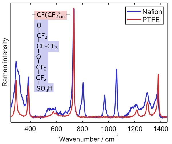
Material characterization with Raman spectroscopy
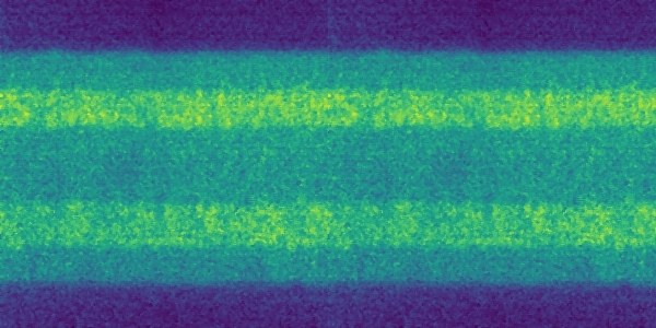
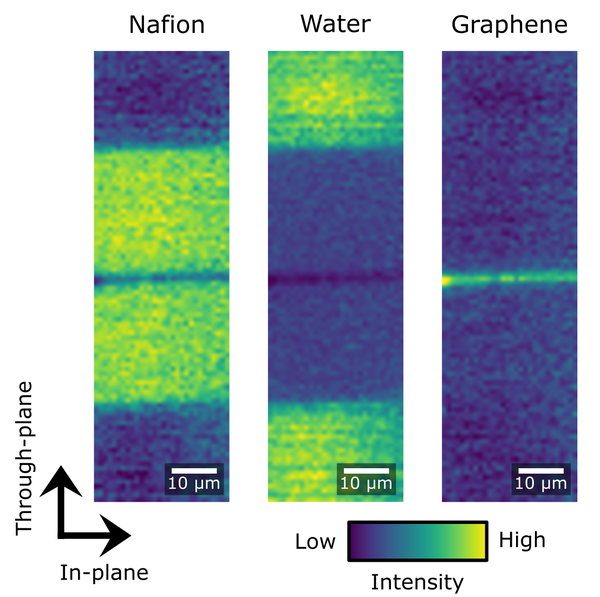
The Raman spectrum of a molecule represents its unique vibrational pattern that is excited upon the interaction with light in the visible spectral range. Vibrational modes of molecules are highly specific for the involved atoms, bond types, and also environmental factors such as the humidification status of the investigated sample. Thus, Raman spectroscopy can be used to identify sample materials and also to characterize properties such as the water uptake of a sample. We employ Raman spectroscopy to analyze the properties of ion exchange polymers like perfluorinated sulfonic acids that are used as proton exchange membranes in fuel cells and water electrolyzers. Confocal Raman microscopy enables a contact-free evaluation of parameters such as membrane thickness, swelling, and chemical degradation during operation.
Focused ion beam scanning electron microscopy
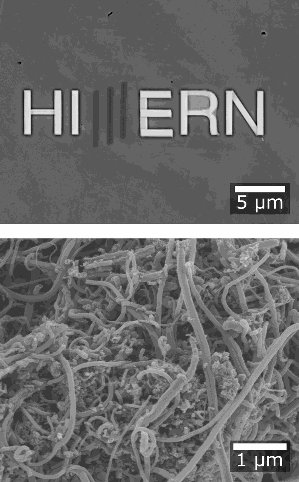
Imaging beyond the diffraction-limited resolution of light microscopy is enabled by electron microscopy. We use a CrossBeam 540 from Zeiss with a Gemini II SEM column, a focused ion beam scanning electron microscope (FIB-SEM). The FIB-SEM is a powerful tool for analyzing the structure and elemental composition of electrochemical samples in a relatively large field of view, ranging from a few millimeters to the nanometer scale. For example, in fuel cell systems, this setup allows us to gain insight into the morphology of the gas diffusion layers, which show relevant features on the micrometer scale and catalyst layers on the nanometer scale. The microscope is equipped with several detectors to gain various information from either secondary electrons, which provide information on the topography of the sample surface, or backscattered electrons that generate image contrast based on differences in the elemental composition of the sample.
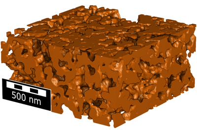
The focused ion beam allows us to modify or mill our specimen surface. This option can be used to mill cross-sectional cuts into the sample for SEM imaging or to perform dedicated sample preparations, like the preparation of thin lamellas for subsequent imaging by transmission electron microscopy. Further, the capability of the microscope to perform milling with its focused ion beam enables FIB-SEM tomography. FIB-SEM tomography is a three-dimensional imaging approach that relies on cycling between SEM imaging the cross-sectional surface of a sample and removing the surface layer with the FIB. By repeating these steps multiple times, a stack of images is generated that shows the inner three-dimensional structure of the sample.
Furthermore, an energy-dispersive X-ray spectroscopy (EDX) detector is installed in the microscope to analyze the elemental composition of a sample in detail. An electron backscatter diffraction detector is available for the microstructural-crystallographic characterization of a specimen. Additional features of our FIB-SEM are micromanipulators, a plasma cleaner, a cryo stage, and a scanning transmission electron microscopy (STEM) detector, which enables high-resolution imaging of very thin samples.